CT Scan Analysis

TOP Metrology is the ideal choice for scanning and X-ray analysis of the various parts supported by the latest generation of industrial tomograph Nikon Metrology, for sub-assemblies and assemblies. Featuring 3 units with the X-ray source of 225kV and 450kV that can cover a wide range of material types and sizes of parts.
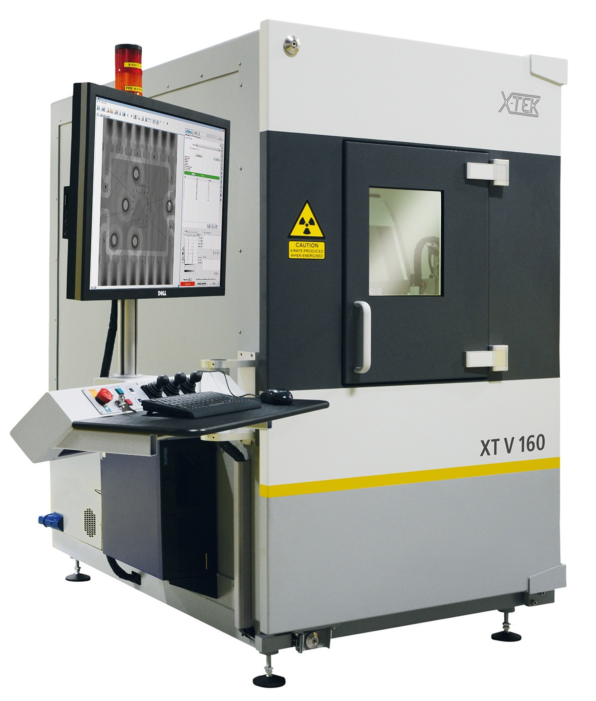
Laboratory TOP Metrology – BucharestComputed tomography Nikon XT V 160
|
Specification: – source 160 kV reflection target – max. power 160W – detector Varian 1313 DX – maximum sample weight 5 Kg |
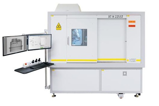
Laboratory TOP Metrology – TimisoaraComputed tomography Nikon XT H 225 ST
|
Specification: – source 225 kV reflection target – max. power 225W – detector 2000 x 2000 pixel ( pixel size = 200 μm) – X travel 450 mm – Y travel 350 mm – Z travel 725 mm – tilt +/- 30 ° – rotate 360 ° – maximum sample weight 50 Kg |
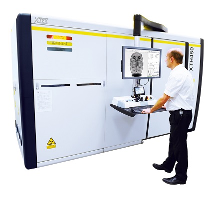
Laboratory TOP Metrology – IasiComputed tomography Nikon XT H 450
|
Specifications: – source 450 kV reflection target – max. power 450W – detector 2000 x 2000 pixel (pixel dimension = 200 μm) – X travel 400 mm – Y travel 600 mm – Z travel 600 mm – rotate 360 ° – maximum sample weight 100 Kg |
Types of analysis:
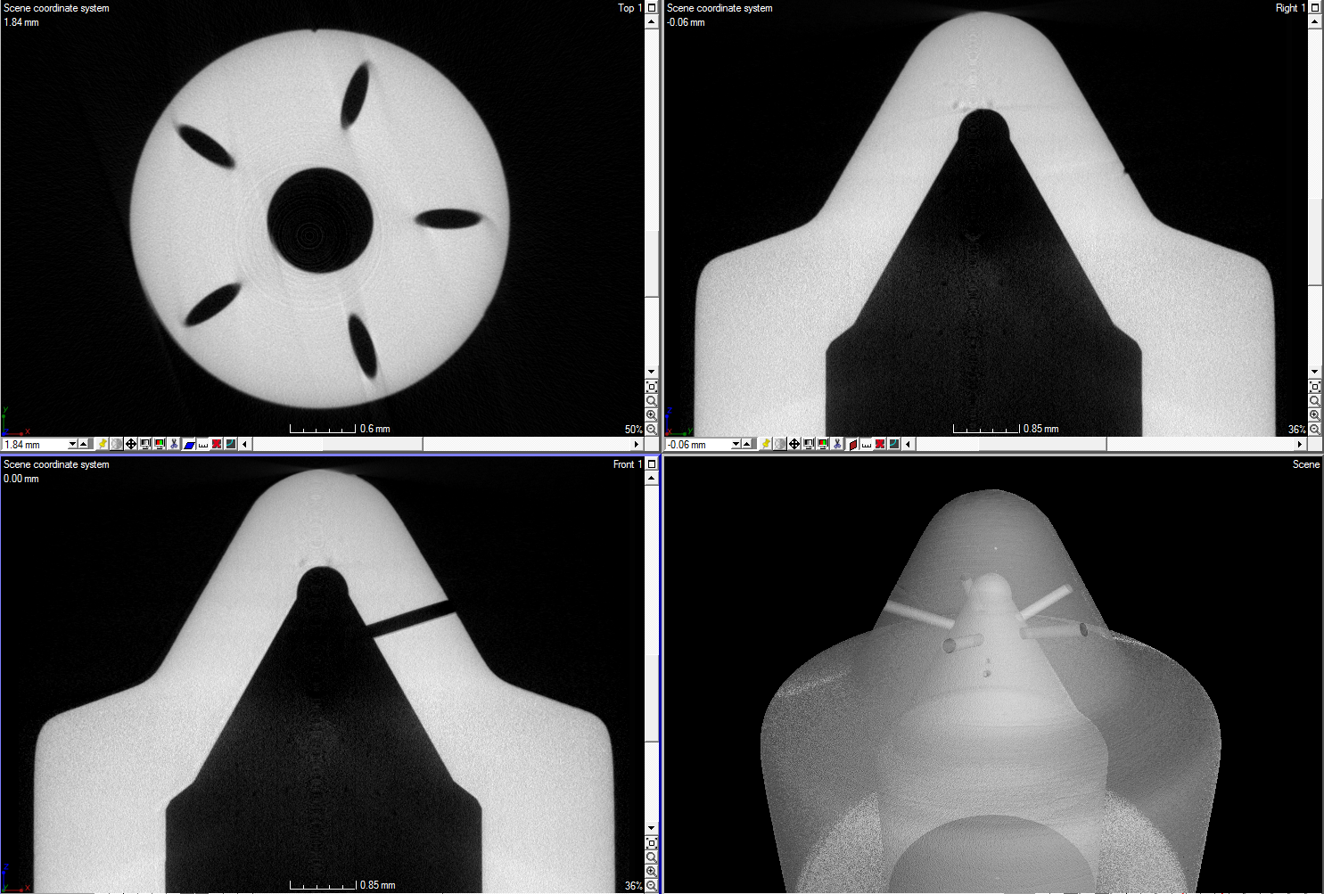
Failure analysis – After scanning are developed three flat section that can be moved through the inside of the part, in order to check any failure witch can appear during manufacture process.
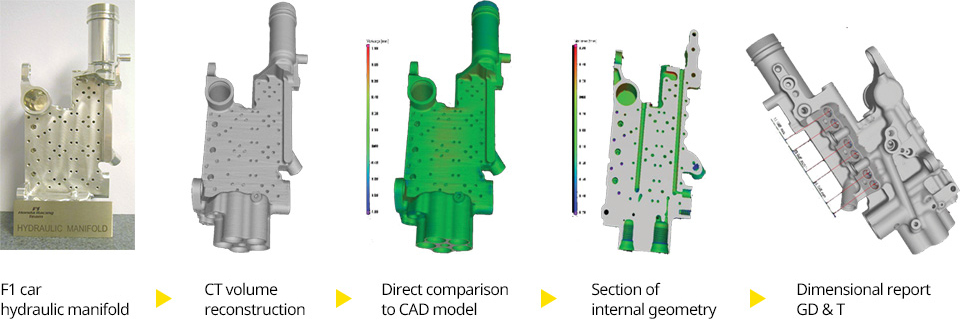
After selecting the desired plan, you can view the interior geometry of the piece accurately.
CAD comparison:
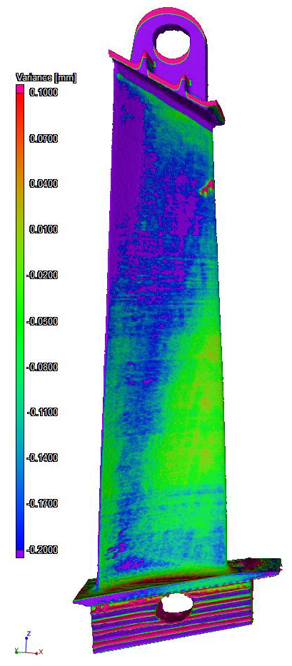
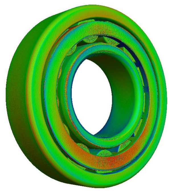
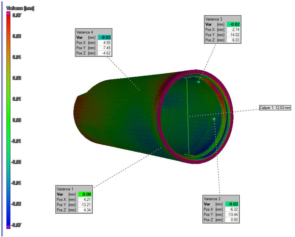
After scanning, the point cloud can be compared to a CAD model. The alignment is performed by a best fit or according to a predetermined coordinate system. The result is displayed as a color map highlighting current deviation against the CAD model geometry both the exterior and the interior.
Porosity / inclusions analysis:
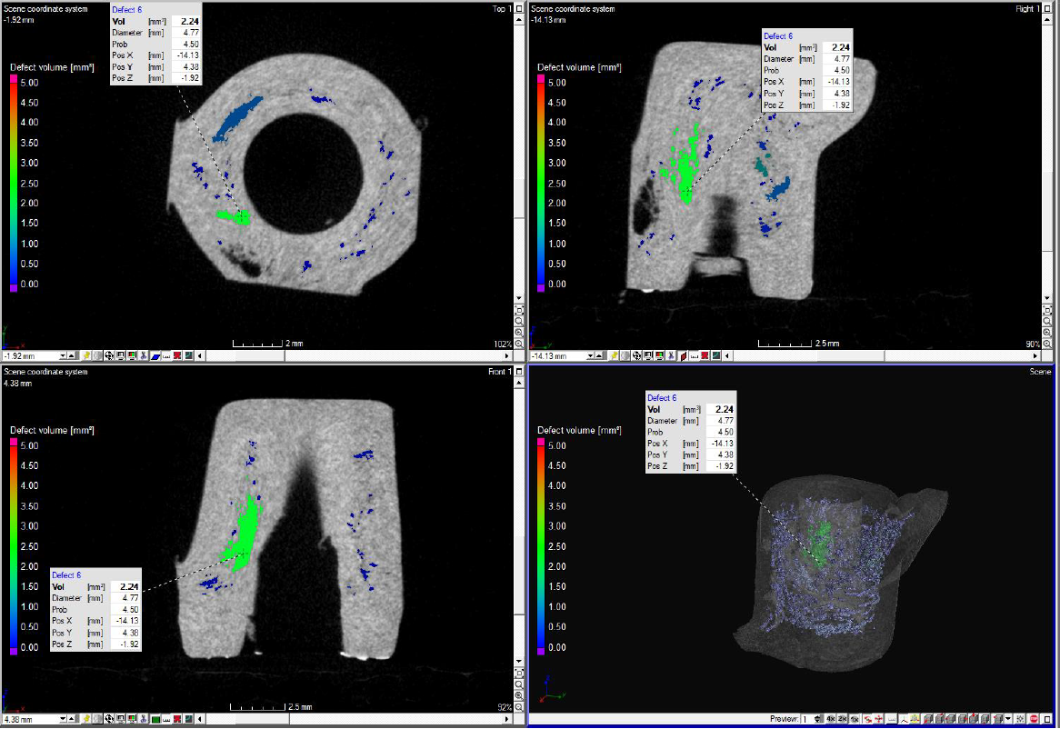
After the scan is done, the software create a bond between every porosity / inclusions detected inside of the part. Every porosity is defined as a volume each one begin represented with a different color according to his dimension. In addition to volume, each void can be identified in coordinates X, Y, Z and individual size. You can determine the percentage of all porosity inside of part.
Wall thickness analysis:
The scanning defines a link between all internal and external surfaces. The distance between each surface is calculated and defined as the minimum thickness of the wall piece. The result is viewed through a color map that shows deviation from an ideal model (CAD). Besides the 3D model displayed as a color map, 2D sections are available for interior surfaces.
Coordinate measurements:
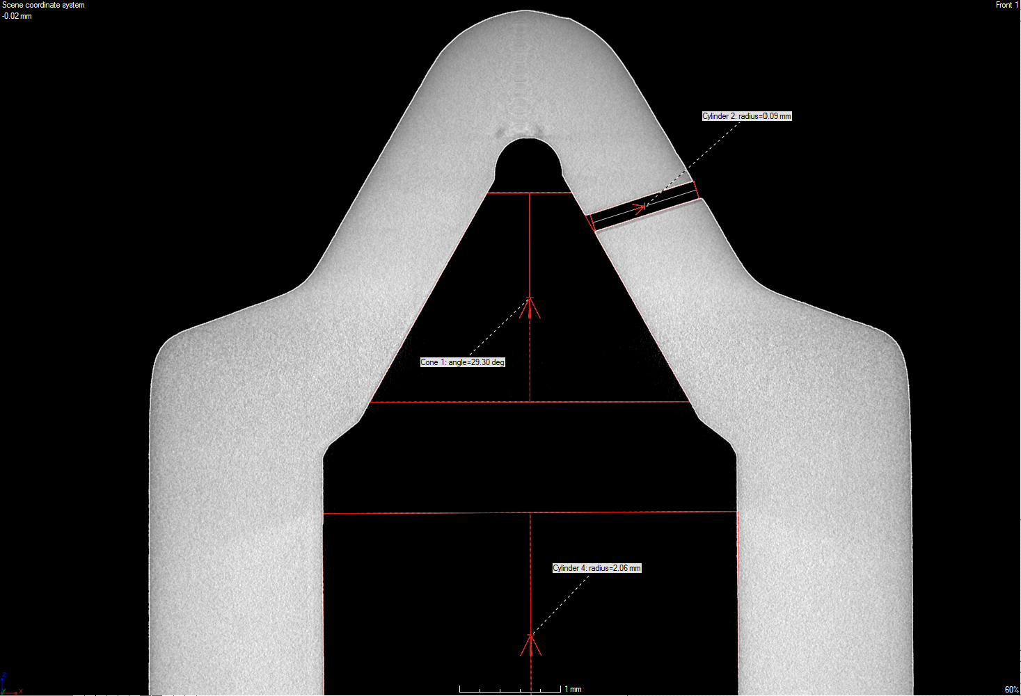
Besides a large variety of types of non-destructive analysis, after scanning is possible to make 3D measurements using the scan. These measurements are valuable for parts with complex surfaces where a laser scanner can not perform the scan.
X-Ray analysis:
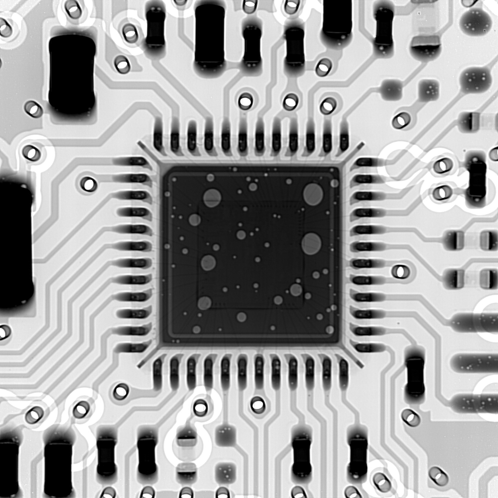
X-ray analysis is defining the fastest control of assemblies and electronic boards. This type of non-destructive analysis is used especially in manufacturing, where time is very important. PCB manufacturing industry is the largest user of x-ray analysis, the main damage occurred during the production of these parts being the appearance of air voids in BGA solder joint and defects in various components on the boards.

