Nikon NWL200

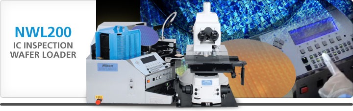
Nikon’s newest and most sophisticated wafer loader for IC inspection microscopes.
The NWL200 series is the first lineup of wafer loaders for inspection microscopes capable of loading 100 micron thin wafers. Thanks to a new chuck system, the NWL200 series achieves highly reliable loading suitable for inspection of next-generation semiconductors. Improved wafer-sensing functions also help prevent damage to wafers, while wafer edge-chipping detection automatically detects edge-chipping defects.
Categories: Semiconductor Equipment
Applications: Wafers
Optional Edge-Chipping Detection
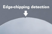
Edge-chipping detection, which was difficult with conventional wafer loaders for microscopes, can now be performed automatically. This enables macro inspections of all areas, adding to the support for inspection of pattern side, back side center, and back side periphery that was already available with earlier models. With high-precision automatic detection, edge defects that cause wafer cracking can be removed promptly.
Remote Access Tool
The loader is equipped with a Web server function. When the loader is connected to a LAN, you can create inspection recipes on a PC and easily backup data from the loader.
Recipe preparation support functions
A Web browser wizard guides you through the steps which are reflected in the NWL200. This allows you to prepare optimum recipes safely and simply, while checking the status of the wafers.
Equipment maintenance
Easily back up and restore inspection recipes.
System Upgrades
Anti-Contamination Measures
To prevent dust arising from friction or impact when centering the wafers, centering and alignment of the orientation flats and notches is performed without contact using photoelectric sensors. The system is configured so as not to interrupt the downflow of clean air in the clean room, and measures are taken to prevent particles arising on the suction surface of the wafer. In addition, the cover is stainless steel to prevent the build-up of static electricity and dust. Every measure has been taken to ensure that today’s highly integrated semiconductor production process is secure from contamination during inspection.
High-Reliability
Should an error occur, an error message is displayed on the LCD panel. Even when the power is turned off, the vacuum chuck of the macro inspection mechanism stays on. If a problem occurs, wafers on the loader can be returned to the carrier without the use of tweezers.
Macro Inspection Functions
In addition to pattern side macro inspections of all areas, macro inspection of the back side periphery and back side center are supported as standard. Macro inspection parameters such as wafer rotation speed and tilt angle can be set automatically or manually. Use the macro setting knobs to preset initial settings and make further adjustments using the joystick. In addition, the new WIL-LED illumination system enables more uniform illumination over a wider area. Various illumination systems are available, from spot lighting to uniform wide area lighting.
Features Geared for Maximum Throughput
Not only is the elevator surprisingly fast, but the non-contact centering mechanism makes it possible to perform alignment quickly and accurately. The multi-arm system also allows loading and unloading of wafers with complete precision, increasing the overall efficiency of transfer and wafer exchange. This dramatically decreases cycle times, achieving levels of throughput never seen before in any other system.
Wafer-Slot Buttons
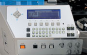
The new wafer-slot buttons on the front panel allow users to select any wafer from its slot with a single button. In addition, the large and prominent LCD panel allows users to set the conditions such as the sampling and inspection patterns, and to check the operating status and the content of errors at a glance. The screens are arranged in a hierarchical structure with one screen for each task, resulting in an intuitive dialog format for smooth progress through the steps. A comprehensive suite of file management functions for carriers, samples and so on is useful for automating inspection.
Modified Design Offers Improved Ergonomics
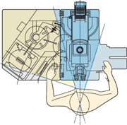
To ensure operation in a natural posture, ergonomic efficiency is designed into every aspect of the system. Operation keys and knobs are located within easy reach of the operator, so that operation requires minimum movement of the hand or eye. The wafer carriers are located at the front and 35° to the left of the operator, making it easy to load carriers and to check the wafers inside the carriers visually.
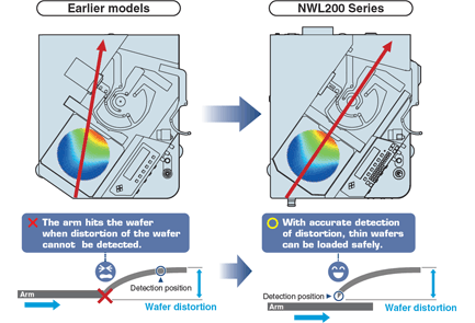
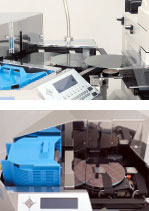
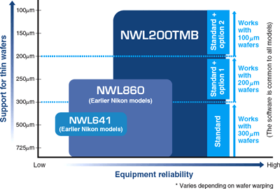
New Chuck System Supports 100µm Wafers
Wafers are getting thinner with advances in manufacturing processes, making it necessary to place very thin wafers on the microscope by hand for inspection at the post-process stage. With Nikon’s new chuck system, the NWL200 Series can load ultra-thin wafers with a thinness of as little as 100µm. This high level of safety and reliability meets all of the requirements for inspection of the latest wafers.
Improved Wafer-Sensing Functions
Since thin wafers can undergo significant distortion in the carrier, the arm may damage them if the position sensors are not accurate. In the past, it was difficult for sensors to read distortion of the wafers accurately, but with optimized arrangement of the wafer sensor beams, the NWL200 Series can accurately detect the shape of thin wafers in the cassette.